Hi,
Hello, first time poster here. I have searched for this board diagram but need some help. I'm repairing a friend's ST70 which has the AVA board installed. The problem is with a component (or possibly several) on the driver board. It would be a help to me if I could get the component layout and/or the schematic. This PC-189a board uses a pair of 6GW8s.
The initial problem with the amp was an "event" that led to the meltdown of one channel's bias sensing resistors. I imagine it was a runaway tube, and it did not help that there was a 20A fuse installed in the amp, which never did blow! Anyway, it was pretty much a charred mess around that tube socket. I have replaced the socket, shrinkwrapped several of the burnt wires and rewired it. The power tubes on that side actually work - I jumped the grids from the good side over to the bad and I do get amplification, but not though that side's driver circuit.
I tried comparing voltage readings from one side of the board
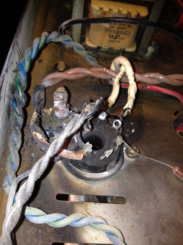
to the other but since they are mirror images I am having a hard time. Hence the request. If anyone can either post a link or attach an image I would be grateful!
Richard